Introduction
The Cell processor consists of a general-purpose POWERPC processor core connected to eight special-purpose DSP cores. These DSP cores, which IBM calls "synergistic processing elements" (SPE), but I'm going to call "SIMD processing elements" (SPE) because "synergy" is a dumb word, are really the heart of the entire Cell concept. IBM introduced the basic architecture of the SPE today, and they're going to introduce the overall architecture of the complete Cell system in a session tomorrow morning.
In this brief overview, I'm first going to talk in some general terms about the Cell approach — what it is, what it's like, what's behind it, etc. — before doing an information dump at the end of the article for more technical readers to chew on and debate. Once the conference is over and I get back to Chicago and get settled in, I'll do some more comprehensive coverage of the Cell.
Back to the future, or, what do IBM and Transmeta have in common?
It seems like aeons ago that I first covered Transmeta's unvieling of their VLIW Crusoe processor. The idea that David Ditzel and the other Transmeta cofounders had was to try and re-do the "RISC revolution" by simplifying processor microarchitecture and moving complexity into software. Ditzel thought that out-of-order execution, register renaming, speculation, branch prediction, and other techniques for latency hiding and for wringing more instruction-level parallelism out of the code stream had increased processors' microarchitectural complexity to the point where way too much die real-estate was being spent on control functions and too little was being spent on actual execution hardware. Transmeta wanted to move register renaming, instruction reordering and the like into software, thereby simplifying the hardware and making it run faster.
I have no doubt that Ditzel and Co. intended to produce a high-performance processor based on these principles. However, moving core processor functionality into software meant moving it into main memory, and this move put Transmeta's designs on the wrong side of the ever-widening latency gap between the execution units and RAM. TM was notoriously unable to deliver on the intitial performance expectations, but a look at IBM's CELL design shows that Ditzel had the right idea, even if TM's execution was off.
IBM's Cell embodies many of the "RISC redivivus" principles outlined above, but it comes at these concepts from a completely different angle. Like TM, IBM started out with the intention of increasing microprocessor performance, but unlike TM, simplifying processor control logic wasn't the magic ingredient that would make this happen. Instead, IBM attacked from the very outset the problem that TM ran headlong into: the memory latency gap. IBM's solution to the memory latency problem is at once both simple and complex. In its most basic form IBM's Cell does what computer architects have been doing since the first cache was invented — Cell moves a small bit of memory closer to the execution units, and lets the processor store frequently-used code and data in that local memory. The actual implementation of this idea is a bit more complicated, but it's still fairly easy to grasp.
Eliminating the Instruction Window
If you've read my series on the Pentium and the PowerPC line or my introduction to basic computer architecture fundamentals, then you're familiar with the concept of an instruction window. I don't want to recap that concept here, so check out this page if you're not familiar with it before moving on.
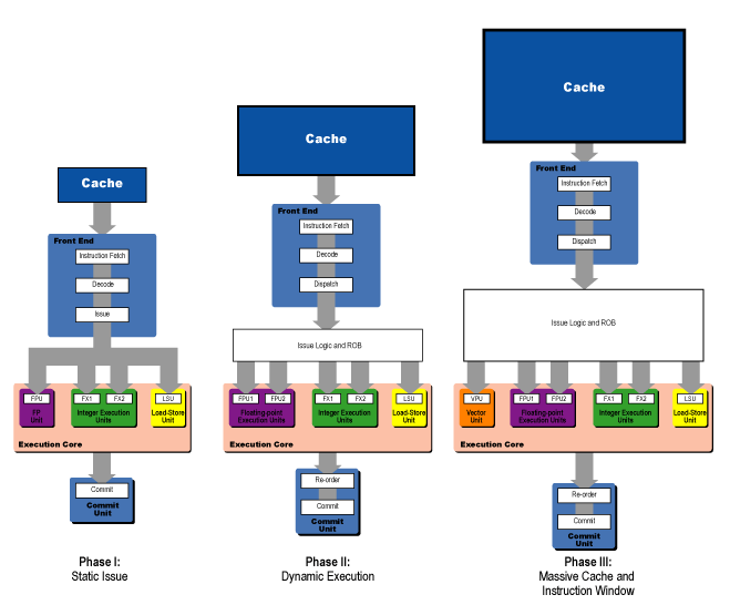
The diagram above shows the development of the microprocessor divided into three phases. The first phase is characterized by static execution, where instructions are issued to the execution units in the exact order in which they're fed into the processor. With dual-issue machines like the original Pentium, two instructions that meet certain criteria can execute in parallel, and it takes a minimal amount of logic to implement this very simple form of out-of-order execution.
In the second phase, computer designers included an instruction window, increased the number of execution units in the execution core, and increased the cache size. So more code and data would fit into the caching subsystem (either L1 or L1 + L2), and the code would flow into the instruction window where it would be spread out and rescheduled to execute in parallel on a large number of execution units.
The third phase is characterized by a massive increase in the sizes of the caches and the instruction window, with some modest increases in execution core width. In this third phase, memory is much farther away from the execution core, so more cache is needed to keep performance from suffering. Also, the execution core has been widened slightly and its units have been more deeply pipelined, with the result that there are more execution slots per cycle to fill.
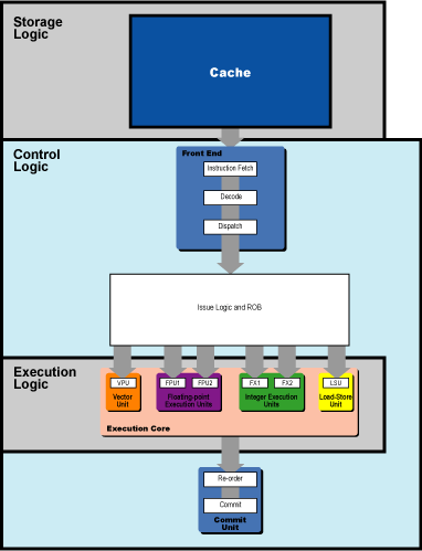
This increased number of execution slots per cycle means that the processor has to find yet more instruction-level parallelism in the code stream, a necessity that gives rise to a massively-increased instruction window (i.e., rename registers, reorder buffer entries, and reservation stations). Now take a look at the diagram below. Notice how the all of that control logic that is associated with the instruction window makes up a huge proportion of the logic in the processor.
Such control logic took up a vanishingly small amount of space in the early static-issue RISC designs like the PPC 601. Of course, back when RISC was first introduced, "control logic" meant "decode logic," since there was no instruction window on those early designs. So RISC reduced the amount of control logic by simplifying the instruction decoding process; this left more room for execution hardware and storage logic in the form of on-die L1 cache.
The end result is that there is this massive amount of control logic that now sits between the processor's cache and its execution core, just as therei s a massive amount of latency that sits between the cache and main memory. This control logic eats up a lot of die space and adds pipeline latency, in return for extracting extra parallelism from the code stream.
Now let's switch gears a moment and look at the issues I raised in my recent Moore's Spring post. The diagram below represents fundamentally the same phenomenon as the diagram in that post, but from a perspective that should look familiar to you.
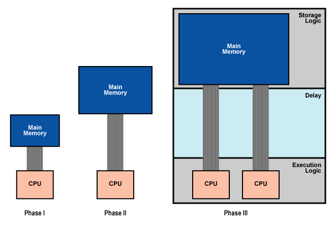
The evolution charted above shows how memory moves further and further away from the execution hardware, while the amount of execution hardware increases (in the form of added processors). What I've tried to illustrate with this diagram and the preceding ones is that there is a homology between the growth of on-die control logic that intervenes between the cache and the execution core and the growth of memory latency. The result is that a trend at the system level is somewhat replicated at the level of the microprocessor. Now let's take a look at a single Cell SPE.
reader comments